Raicol Crystals (Raicol)
高品質 非線形結晶
ワンストップショップ。 結晶成長から光学アッセンブリまで。
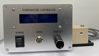
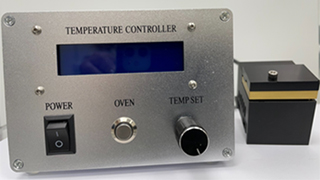
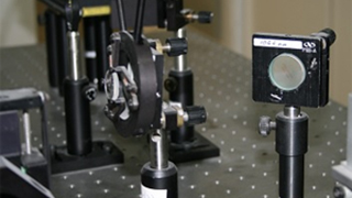
Raicol Crystals社(以下 Raicol社)は、レーザーシステム用の高品質な非線形光学結晶、およびRTP高速ポッケルスセル(最大1.2MHz)のメーカーです。
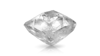
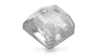
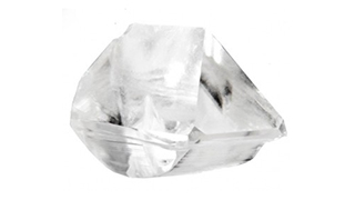
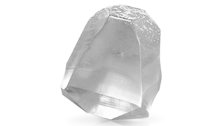
フラックス法で成長させた、グレートラックに高い耐性を持つ KTP結晶を、世界で初めて開発しました。
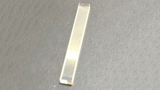
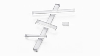
Raicol社では、RTP、KTP、LBO、BBO、PPKTP、PPSLT、PPLN、CLBOを含む様々な結晶を製造しています。
最先端の製造施設はワンストップショップで、高品質な生産に必要な独自の結晶成長システム、切断 ・ 研磨機、X線測定システム、クリーンルーム、
光学組立機器、最先端のテストステーション、コーティング設備(IBS方式)を備えています。
製品ラインアップ
量子光素子


周波数変換
非線形周波数変換とは、光学的非線形性を利用して、入力光の光パワーの一部を別の波長領域の出力光へ変換する技術です。