
Polymer-Wrapped ナノチューブ
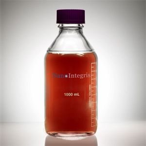
IsoSol-S100®
The use of specialized patent-pending dialkyl homopolymers developed by the National Research Council of Canada, within the Printable Electronics Program, has enabled us to disperse and extract single-walled carbon nanotubes to the highest levels of semiconducting enrichment and purity to date: IsoSol-S100. The starting materials are the purified and highly-scalable RF-plasma grown carbon nanotube supplied by Raymor Nanotech *1.
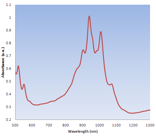
UV-Vis-NIR spectrophotometric assessment of purity *2 indicate that this material has semiconducting purities at or greater than 99.9% with the metrics of Itkis Ratio *3 and Phi Values *4 exceeding 0.5 and 0.4, respectively.
The highly graphitized starting material and low sonication intensity utilized for the extraction technique minimizes damage to the nanotubes, allowing the material to exhibit high crysallinity and longer average lengths of 2µm, not previously seen when utilizing DGU *5 or Chromatography-based *6 separation methods.
Additionally, the material is processed in organic solvent with a polymer : nanotube ratio that can be adjusted to less than a factor of four (surfactant : nanotube ratio is 1x10³ in our aqueous surfactant solutions). The solutions also display stabilities of greater than six months. These properties promote great nanotube deposition and adhesion for device creation.
Experimentally, thin film transistors have been prepared from the IsoSol-S100 material on SiO2/Si substrates *7, leading to average mobilities exceeding 27cm2/(Vs) and On/Off ratios of 1.8x10⁶. These properties allow the material to be well-suited for ink jet and aerosol jet printing.
-
*1K. S. Kim, A. Moradian, J. Mostaghimi, Y. Alinejad, A. Shahverdi, B. Simard and G. Soucy, Nano Research, 2009, 2, 800.
-
*2M. Ouyang , J. Huang , and C.M. Lieber, Acc. Chem. Res. , 2002, 35 (12), 1018-1025.
-
*3J. Chen, A.M. Rao, S. Lyuksyutov, M.E. Itkis, M.A. Hamon, H. Hu, R.W. Cohn, P.C. Eklund, D.T. Colbert, R.E. Smalley, and R.C. Haddon, J. Phys. Chem. B, 2001, 105 (13), 2525–2528.
-
*4K.S. Mistry, B.A. Larsen, and J.L. Blackburn, ACS Nano, 2013, 7, 2231-2239.
-
*5M.S. Arnold, A.A. Green, J.F. Hulvat, S.I. Stupp, and M.C. Hersam, Nat. Nanotechnol., 2008, 3, 387, 394.
-
*6M. Zheng and E.D. Semke, J. Am. Chem. Soc., 2007, 129, 6084-6085.
-
*7J. Ding, Z. Li, J. Lefebvre, F. Cheng, G. Dubey, S. Zou, P. Finnie, A. Hrdina, L. Scoles, G.P. Lopinski, C. T. Kingston, B. Simard, and P.R.L. Malenfant, Nanoscale, 2014, 6, 2328-2339.
仕様
| Optical Purity | >99.9% |
|---|---|
| Itkis Ratio (Ї) | >0.5 |
| Phi Value (Φ) | >0.39 |
| Nanotube Concentration | >0.01mg/mL |
| Surfactant : Nanotube Concentration | <4 |
| Standard Solvent Media | Toluene |
| Shelf Life | 6~9 months |
SEM and AFM
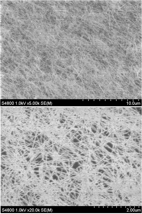
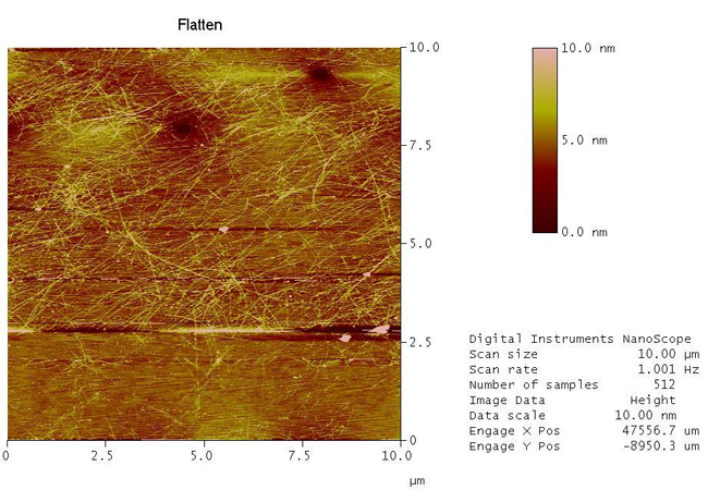
mages used by permission of H. Chen: Nanotechnology Research Laboratory, Department of Electrical Engineering,University of Southern California.
| 直径範囲 | 1.2~1.4nm |
|---|---|
| 平均長 | 2 µm |
Raman
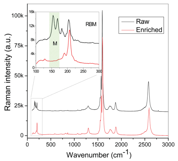
Image used by permission of P. Malenfant: Security and Disruptive Technologies Portfolio,National Research Council Canada.
The Radical Breath Mode (RBM) of the spectra excited at 785nm shows that the IsoSol-S100 material has a nearly flat baseline in the metallic region from 145 to 175 cm-1, indicative of a high semiconducting purity.
| Metal Catalyst Impurity | <0.5 % |
|---|---|
| Amorphous Carbon Impurity | <1 % |
PLE Map
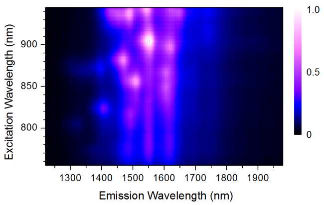
Image used by permission of P. Malenfant: Security and Disruptive Technologies Portfolio,National Research Council Canada.
A photoluminescence excitation (PLE) map for the IsoSol-S100 material shows well resolved (S22, S11) maxima,indicative of well separated nanotubes. UP to 19 (n,m) species contribute to the spectrum,with 8 or 9 having peak intensities higher than or close to 0.5.
The (10,9) chirality peak with S11=1570nm and S22=910nm, proved to be the strongest.
技術資料
データシート
この製品に関するお問合せフォーム
フォームが表示されるまでしばらくお待ちください。
しばらくお待ちいただいてもフォームが表示されない場合、恐れ入りますが こちら までお問合せください。